On-Chip Measurements in High-Speed System Environments:
RF-contacting and fiber coupling of research stage devices for system tests
In order to test research stage devices we offer electrical and optical characterization of photo diodes and edge emitting as well as surface emitting laser diodes. We carry out chip-level high frequency RF-contacting and stable fiber coupling for tests in system environments.
Featured Measurement Types
DC Characterization
- L-I-V curves
- Derivation of series resistance
- Optical spectra
- Temperature behavior (20 °C to 200 °C)
RIN- and Jitter Measurements
- Relative intensity noise and jitter derived from electrical spectrum
Small-Signal Measurements
S11 and S21 parameters including
- Small-signal frequency bandwidth
- RF-matching of the device under test
- Resonance behavior of intrinsic processes (relaxation oscillation frequency)
Large-Signal Measurements
- Eye diagrams (Q-factor, extinction ratio, bit patterning)
- Bit-error ratio measurements as a function of the optical signal-to-noise ratio or the received power up to 50 GBd and for different modulation formats
- Transmission experiments using single-mode or multimode fiber links
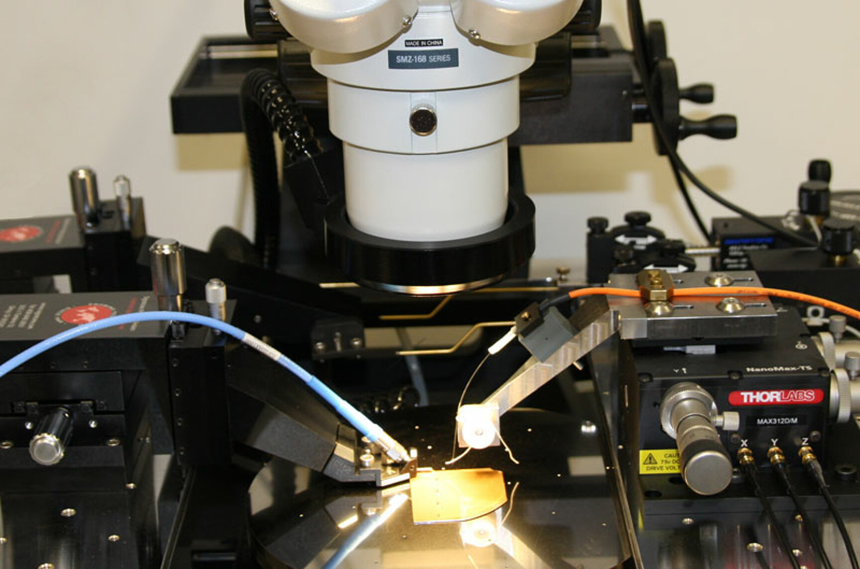
Features of Probe Station Setup
- Electrical DC- and RF-probing up to 50 GHz
- Optical fiber coupling, optical feedback for stabilization, precision in micrometer range
- Temperature controlled (20 °C up to 120 °C)
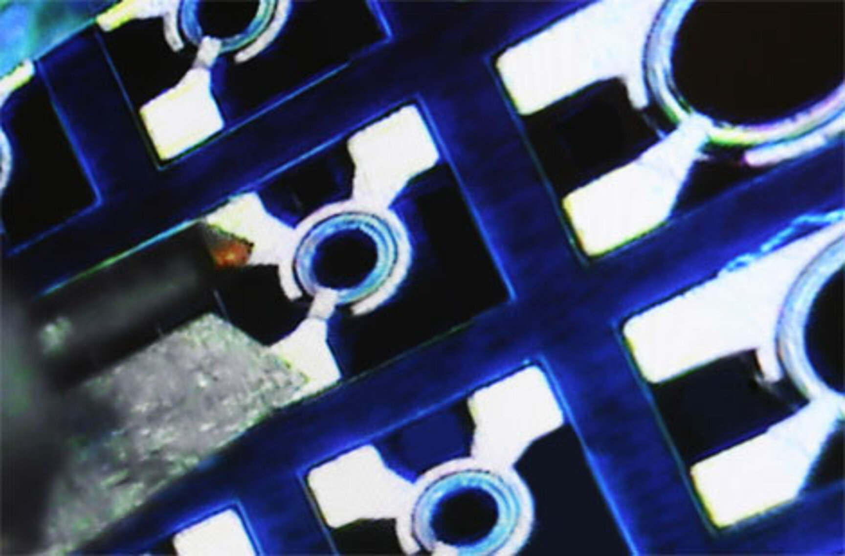
- Microscope images of chip surface
